
Foreign lithography and wafer processing equipment manufacturers have experienced a significant decline in sales within China. In 2024, China accounted for 41% of ASML’s revenue, but this proportion fell to 33% in 2025 and is projected to shrink to 20% in 2026. This decline mirrors similar trends seen with American company Applied Materials, whose sales in China decreased from 37% of total revenues in 2024 to 30% in 2025.
Other American companies like Lam Research and KLA, along with Japan’s Tokyo Electron, have also witnessed drops in their Chinese sales during 2025 compared to 2024. This trend stems from two primary factors: first, U.S. sanctions restrict American and allied manufacturers from exporting advanced machines to Chinese clients; second, the Chinese government is championing the adoption of domestically produced equipment in its semiconductor manufacturing facilities. By 2025, Chinese-made tools comprised 35% of semiconductor equipment usage, with a goal of reaching 50% in new factories by 2026, underscoring China’s ambition for technological independence amid ongoing tensions with the U.S.
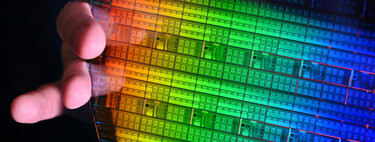
China’s Progress in the Semiconductor Sector
China has significantly advanced in the semiconductor sector, supported by substantial governmental investment in domestic manufacturing capabilities. Companies are now competing with foreign counterparts in areas like deposition, thermal processing, etching, and wafer cleaning. However, China still lacks domestic extreme ultraviolet (EUV) photolithography machines, which are critical for producing more advanced microchips. The development of these machines is anticipated by the end of the decade, but until then, this remains a significant vulnerability for China’s chip industry.
Among the noteworthy Chinese firms is Pulin Technology, which, along with others like Naura Technology and AMEC (Advanced Micro-Fabrication Equipment Inc. China), is developing its own state-of-the-art photolithography machines. Mid-2025 saw Pulin deliver its first advanced equipment utilizing nanoimprint lithography (NIL) technology to a client.
Understanding Nanoimprint Lithography
NIL is not a new concept; the Japanese company Canon has offered commercial NIL solutions for years, and Pulin’s designs share similar operational principles. Though NIL technology is positioned as an alternative to ASML’s EUV machines, it is not yet a replacement for the high-aperture versions, the most advanced and costly in the market.
Producing silicon wafers with EUV technology involves precise alignment of the geometric pattern from the mask to the silicon surface using ultraviolet light and intricate optical elements. In contrast, NIL lithography can transfer patterns without the need for complex optical systems, making it simpler and more affordable but slower due to multiple sequential processes.
Cost Comparisons and Future Prospects
Canon claims its NIL technology can produce integrated circuits similar to those made with ASML’s EUV machines, potentially reaching 2nm chip production in the future. With a price tag of approximately $15 million per NIL machine—ten times less than ASML’s EUV models, priced at around $150 million—Pulin’s NIL machines will likely fall within a comparable range.
This period of innovation and advancement in China’s chip manufacturing sector, alongside government support, signals a notable shift in the global semiconductor landscape.
For more insights, visit Tom’s Hardware.