Integrated 2 nm circuits are on the brink of revolutionizing the semiconductor market. While users are aware that nanometers have lost much of their original significance, representing merely a category of semiconductors, they no longer accurately reflect physical parameters such as the distance between transistors or the actual dimensions of logical gates. Each chip manufacturer employs these measures with considerable flexibility, allowing for direct comparisons of the lithographs they attempt to sell us.
As the competition heats up, TSMC, Intel, and Samsung are gearing up for an intense showdown to capture as many customers as possible for their 2 nm or equivalent node lines. The ultimate victor in this battle will undoubtedly be the Dutch company ASML . They are the sole producers on Earth of the extreme ultra-violet (EUV) photolithography equipment essential for surpassing 2 nm technology and achieving optimal performance.
According to Digitimes Asia, Samsung’s semiconductor division is contemplating increasing its acquisition of high-NA EUV machines from ASML. This decision directly relates to their strategy to mitigate the technological and commercial gap between themselves and TSMC, which currently commands nearly 60% of the chip market. Although high-NA EUV machines remain in the testing phase, there’s little doubt they will become the centerpiece of the semiconductor industry by 2026 and beyond.
ASML’s High-NA Lithography Machinery: An Engineering Marvel
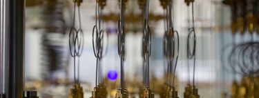
The sophisticated Twinscan Exe: 5000 lithography systems produced by ASML are unprecedented in the field of integrated circuit manufacturing. Weighing as much as two Airbus A320s, these machines comprise over 100,000 components, 3,000 cables , 40,000 bolts , and more than 2 kilometers of electrical connections. Such intricate engineering results in one of the most expensive pieces of technology ever made, with the latest unit costing approximately 350 million euros. This price may lead some chip manufacturers to reconsider their purchasing decisions.
ASML plans to deliver around 20 high-NA EUV machines annually starting in 2025 .
ASML engineers have dedicated over a decade to developing the technology that underpins these machines, representing a significant advancement in second-generation extreme EUV lithography . Starting from 2025 , ASML intends to provide customers with 20 high-NA EUV systems each year , allowing them to manufacture chips at 2 nm and beyond. A notable feature of this machine is its advanced optical architecture, which boasts an NA of 0.55 , compared to the 0.33 of first-generation EUV equipment.
The refined optical capabilities enhance the resolution of patterns transferred onto silicon wafers, enabling the production of chips utilizing cutting-edge integration technologies, surpassing those currently employed in 3 nm nodes . Additionally, ASML has refined the mechanical systems responsible for wafer handling, ensuring that a single EUV machine can produce over 200 wafers per hour .
The complexities and technical sophistication of these systems underscore the collaborative efforts of various companies, including Zeiss , a German optical technology firm, and Cymer , an American company integral to ASML’s structure. Cymer provides the essential ultraviolet light required for the photolithography process, enabling the precise transfer of geometric patterns described by masks to silicon wafers.
Image credit: ASML
For more information, check out Digitimes Asia.
As we look ahead, the competition among TSMC, Intel, and Samsung will reshape the semiconductor landscape, with ASML playing a pivotal role in driving the next wave of technological innovation. The advancements in 2 nm circuitry and high-NA lithography machines promise to not only enhance chip performance but also redefine what is possible in computing technology. With firms continually investing in advanced machinery, we can expect significant strides in efficiency and capability in the semiconductor industry.